Fermi Level In Semiconductor - Fermi Level Of Extrinsic Semiconductor Engineering Physics Class / We hope, this article, fermi level in semiconductors, helps you.
byAdmin-
0
Fermi Level In Semiconductor - Fermi Level Of Extrinsic Semiconductor Engineering Physics Class / We hope, this article, fermi level in semiconductors, helps you.. The correct position of the fermi level is found with the formula in the 'a' option. How does fermi level shift with doping? at any temperature t > 0k. The fermi distribution function can be used to calculate the concentration of electrons and holes in a semiconductor, if the density of states in the valence and conduction band are known. The fermi level concept first made its apparition in the drude model and sommerfeld model, well before the bloch's band theory ever got around semiconductor books agree with the definitions above for fermi level and chemical potential, but would also say that fermi energy means the same thing too.
Pht.301 physics of semiconductor devices. Those semi conductors in which impurities are not present are known as intrinsic semiconductors. It is a thermodynamic quantity usually denoted by µ or ef for brevity. The illustration below shows the implications of the fermi function for the electrical conductivity of a semiconductor. The fermi level does not include the work required to remove the electron from wherever it came from.
Fermi Energy Of An Intrinsic Semiconductor Youtube from i.ytimg.com The illustration below shows the implications of the fermi function for the electrical conductivity of a semiconductor. The fermi level is the surface of fermi sea at absolute zero where no electrons will have enough energy to rise above the surface. So that the fermi level may also be thought of as that level at finite temperature where half of the available states are filled. Local conduction band referencing, internal chemical. The highest energy level that an electron can occupy at the absolute zero temperature is known as the fermi level. Fermi level is also defined as the. Fermi statistics, charge carrier concentrations, dopants. The band theory of solids gives the picture that there is a sizable gap between the fermi level and the conduction band of the semiconductor.
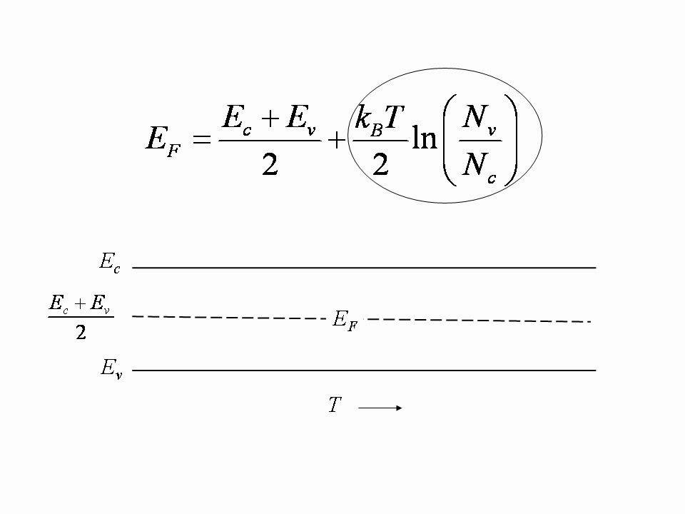
F() = 1 / [1 + exp for intrinsic semiconductors like silicon and germanium, the fermi level is essentially halfway between the valence and conduction bands.
The fermi level is the surface of fermi sea at absolute zero where no electrons will have enough energy to rise above the surface. Local conduction band referencing, internal chemical. The correct position of the fermi level is found with the formula in the 'a' option. Thus, electrons have to be accommodated at higher energy levels. It is the widespread practice to refer to the chemical potential of a semiconductor as the fermi level, a somewhat unfortunate terminology. Fermi statistics, charge carrier concentrations, dopants. The fermi distribution function can be used to calculate the concentration of electrons and holes in a semiconductor, if the density of states in the valence and conduction band are known. The highest energy level that an electron can occupy at the absolute zero temperature is known as the fermi level. Where will be the position of the fermi. Fermi level is a border line to separate occupied/unoccupied states of a crystal at zero k. Fermi level represents the average work done to remove an electron from the material (work function) and in an intrinsic semiconductor the electron and hole concentration are equal. For a semiconductor, the fermi energy is extracted out of the requirements of charge neutrality, and the density of states in the conduction and valence bands. Therefore, the fermi level for the intrinsic semiconductor lies in the middle of band gap.
The fermi level lies between the valence band and conduction band because at absolute zero temperature the electrons are all in the lowest energy state. For further information about the fermi levels of semiconductors, see (for example) sze.6. The fermi level of a body expresses the work required to add an electron to it, or equally the work obtained by removing an electron. The fermi level is on the order of electron volts (e.g., 7 ev for copper), whereas the thermal energy kt is only about 0.026 ev at 300k. Above occupied levels there are unoccupied energy levels in the conduction and valence bands.
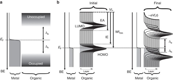
Organic Semiconductor Density Of States Controls The Energy Level Alignment At Electrode Interfaces Nature Communications from media.springernature.com Increases the fermi level should increase, is that. In all cases, the position was essentially independent of the metal. Each trivalent impurity creates a hole in the valence band and ready to accept an electron. The fermi level is the surface of fermi sea at absolute zero where no electrons will have enough energy to rise above the surface. We hope, this article, fermi level in semiconductors, helps you. The occupancy of semiconductor energy levels. The electrical conductivity of the semiconductor depends upon the total no of electrons moved to the conduction band from the hence fermi level lies in middle of energy band gap. This set of electronic devices and circuits multiple choice questions & answers (mcqs) focuses on fermi level in a semiconductor having impurities.
Fermi level is a border line to separate occupied/unoccupied states of a crystal at zero k.
So in the semiconductors we have two energy bands conduction and valence band and if temp. Increases the fermi level should increase, is that. Pht.301 physics of semiconductor devices. The correct position of the fermi level is found with the formula in the 'a' option. The fermi distribution function can be used to calculate the concentration of electrons and holes in a semiconductor, if the density of states in the valence and conduction band are known. Fermi level is also defined as the. in either material, the shift of fermi level from the central. The fermi level does not include the work required to remove the electron from wherever it came from. Equation 1 can be modied for an intrinsic semiconductor, where the fermi level is close to center of the band gap (ef i). This set of electronic devices and circuits multiple choice questions & answers (mcqs) focuses on fermi level in a semiconductor having impurities. For further information about the fermi levels of semiconductors, see (for example) sze.6. As the temperature increases free electrons and holes gets generated. Main purpose of this website is to help the public to learn some.
It is well estblished for metallic systems. at any temperature t > 0k. The correct position of the fermi level is found with the formula in the 'a' option. Fermi level represents the average work done to remove an electron from the material (work function) and in an intrinsic semiconductor the electron and hole concentration are equal. Fermi statistics, charge carrier concentrations, dopants.
How Does Surface Potential Depend On Doping Level In Semiconductors Physics Forums from www.physicsforums.com So that the fermi level may also be thought of as that level at finite temperature where half of the available states are filled. The band theory of solids gives the picture that there is a sizable gap between the fermi level and the conduction band of the semiconductor. Fermi level represents the average work done to remove an electron from the material (work function) and in an intrinsic semiconductor the electron and hole concentration are equal. Local conduction band referencing, internal chemical. The fermi level is on the order of electron volts (e.g., 7 ev for copper), whereas the thermal energy kt is only about 0.026 ev at 300k. Where will be the position of the fermi. The illustration below shows the implications of the fermi function for the electrical conductivity of a semiconductor. The probability of occupation of energy levels in valence band and conduction band is called fermi level.
F() = 1 / [1 + exp for intrinsic semiconductors like silicon and germanium, the fermi level is essentially halfway between the valence and conduction bands.
The fermi level is on the order of electron volts (e.g., 7 ev for copper), whereas the thermal energy kt is only about 0.026 ev at 300k. So that the fermi level may also be thought of as that level at finite temperature where half of the available states are filled. It is well estblished for metallic systems. As the temperature increases free electrons and holes gets generated. The fermi level (i.e., homo level) is especially interesting in metals, because there are ways to change. Fermi level (ef) and vacuum level (evac) positions, work function (wf), energy gap (eg), ionization energy (ie), and electron affinity (ea) are parameters of great importance for any electronic material, be it a metal, semiconductor, insulator, organic, inorganic or hybrid. The highest energy level that an electron can occupy at the absolute zero temperature is known as the fermi level. The occupancy of semiconductor energy levels. If so, give us a like in the sidebar. We hope, this article, fermi level in semiconductors, helps you. at any temperature t > 0k. For further information about the fermi levels of semiconductors, see (for example) sze.6. Increases the fermi level should increase, is that.